PARADIM Highlight #94—Local User Project (2024)
Judy Cha (local user, Cornell), Lena F. Kourkoutis & Eun-Ah Kim (PARADIM, Cornell)
Quantum materials are of fundamental and technological interest, with potential applications ranging from quantum computers to next-generation microelectronics. An exciting property of layered quantum materials like tantalum sulfide (TaS2) are charge density waves (CDW)—emergent periodic modulations of the electron density. TaS2 hosts several CDW states that spontaneously break crystal symmetries, mediate metal-insulator transitions, and compete with superconductivity, but are also challenging to visualize on the nanoscale. Quantum materials are commonly studied with bulk averaging probes and thus their nanoscale properties are poorly understood.
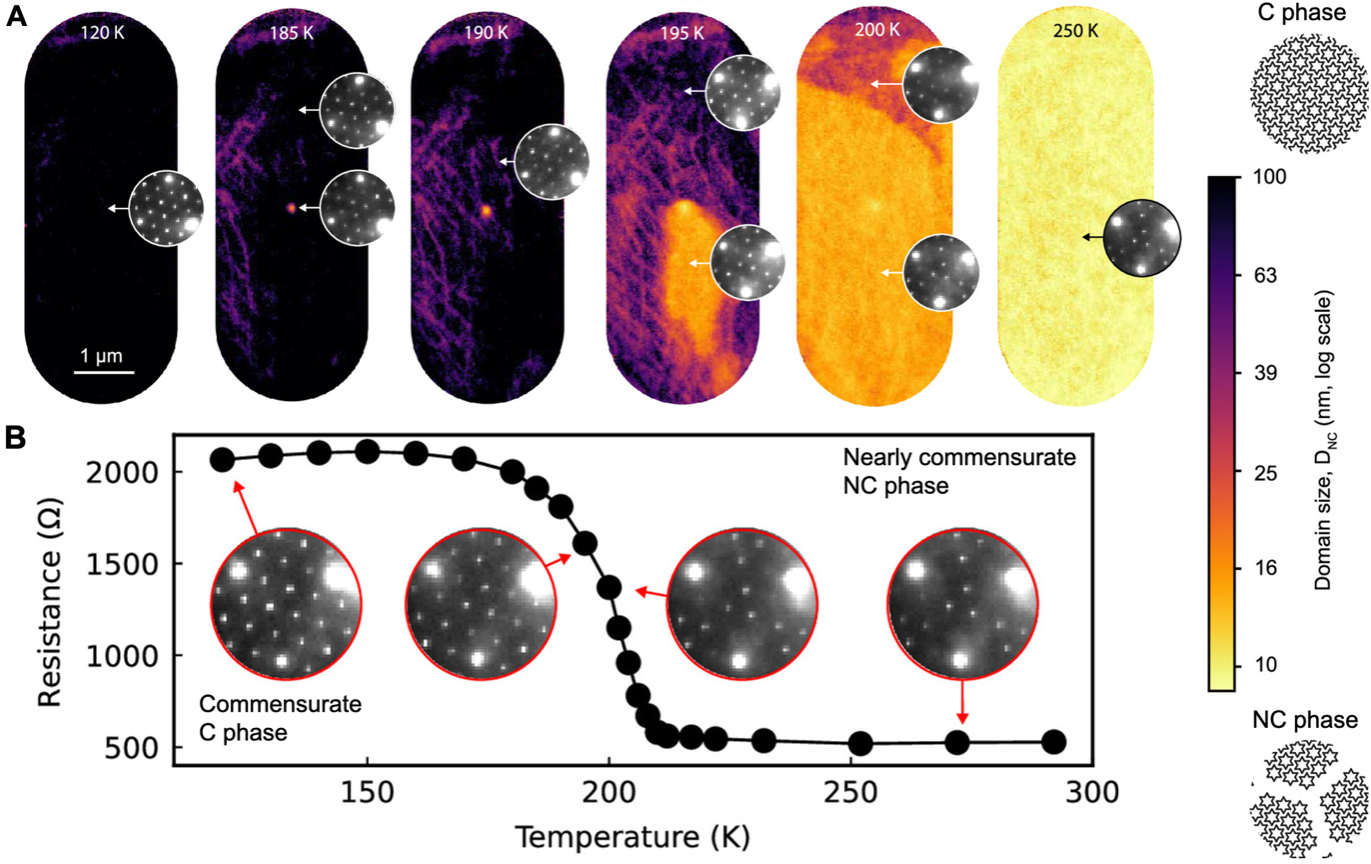
Figure 1: CDW phase transition during warming experiment. (A) 4D-STEM derived maps, color-coded for the domain size DNC for select temperatures. Insets show extracted diffraction data. (B) The electrical resistance measured during the in situ 4D-STEM experiment upon warming.
Here, PARADIM’s development of real-time temperature control during cryogenic scanning transmission electron microscopy has enabled its users to image the CDW transition while altering temperature and electric field. Unsupervised machine learning is applied to cluster the five-dimensional, terabyte scale microscopy datasets, and demonstrates a one-to-one correlation between device resistance, CDW phase, and the material microstructure. The team shows that basal dislocations—which are ubiquitous in 2D materials—both nucleate and pin the CDW transition and locally alter the transition temperature (Tc) by nearly ~75 K. Further, the team shows that the dislocation density can be used to engineer device properties.
This study of the coupled charge density wave (CDW) and insulator-to-metal transitions in the 2D quantum material 1T-TaS2 combined in situ cryogenic 4D scanning transmission electron microscopy with in situ electrical resistance measurements, to directly visualize the CDW transition and establish that the transition is mediated by basal dislocations (stacking solitons). The observed dislocations can both nucleate and pin the transition and locally alter the transition temperature Tc by nearly ~75 K. This finding was enabled by the application of unsupervised machine learning to cluster five-dimensional, terabyte scale datasets, which demonstrate a one-to-one correlation between resistance—a global property—and local CDW domain-dislocation dynamics, thereby linking the material microstructure to device properties. This work represents a major step toward defect-engineering of quantum materials, which will become increasingly important as we aim to utilize such materials in real devices.
The study of 2D transition metal dichalcogenides (TMDs) has largely assumed that the layer stacking in the nanoscale limit adopts one or more of the possible precise stacking sequences found in bulk specimens. This work demonstrates – via atomic resolution imaging – that in fact much greater stacking complexity arises in the thin limit than previously assumed. Given the importance of interlayer stacking on electronic, magnetic, and optical properties, this result suggests greater study of stacking is needed during the characterization of 2D TMDs.
PARADIM’s user facility for electron microscopy at Cornell University provided access to high-resolution STEM capabilities including advanced sample preparation, to visualize the inter-layer stacking and map out how it changes as a function of temperature in relation to the defects (in particular dislocations) in the sample.
Featured story in the Cornell Chronicle: https://news.cornell.edu/stories/2024/08/kourkoutis-cryo-imaging-continues-drive-quantum-discoveries.
J.L. Hart, H. Pan, S. Siddique, N. Schnitzer, K. Mallayya, S. Xu, L.F. Kourkoutis, E.-A. Kim, and J.J. Cha, "Real-Space Visualization of a Defect-Mediated Charge Density Wave Transition," Proc. Natl. Acad. Sci. U.S.A. 121, e2402129121 (2024).
The in situ four-dimensional scanning transmission electron microscopy and machine learning analysis were supported by the Department of Energy, Basic Energy Sciences DE-SC0023905. The computation was carried out on the cluster supported by the Gordon and Betty Moore Foundation’s Emergent Phenomena in Quantum Systems Initiative, Grant GBMF10436 to Eun-Ah Kim. N.S. acknowledges support from the NSF Graduate Research Fellowships Program under Award No. DGE-2139899. H.P. was supported by the NSF [platform for the accelerated realization, analysis, and discovery of interface materials (PARADIM)] under Cooperative Agreement No. DMR-2039380. K.M. was supported by Eric and Wendy Schmidt AI in Science Postdoctoral Fellowship: A Schmidt Futures program. Device fabrication was performed in part at the Cornell NanoScale Facility, a member of the National Nanotechnology Coordinated Infrastructure, which is supported by the NSF (Grant NNCI-2025233). This work made use of the electron microscopy facility of PARADIM, which is supported by the NSF under Cooperative Agreement No. DMR-2039380, and the Cornell Center for Materials Research Shared Facilities which are supported through the NSF Materials Research Science and Engineering Centers Program (DMR-1719875). The Titan Themis 300 was acquired through NSF-MRI-1429155, with additional support from Cornell University, the Weill Institute and the Kavli Institute at Cornell.
Data Availability: Access to data is provided through the PARADIM Data Collective at https://doi.org/10.34863/0k5x-w691.