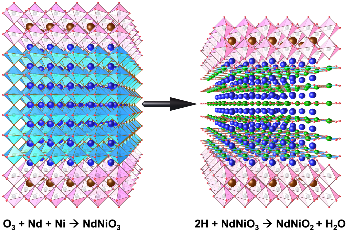
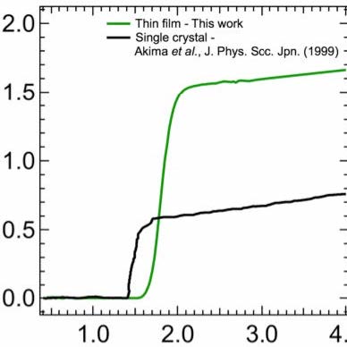
Simplified (and superior!) Synthesis of Nickelate Superconductors (MIP #91)
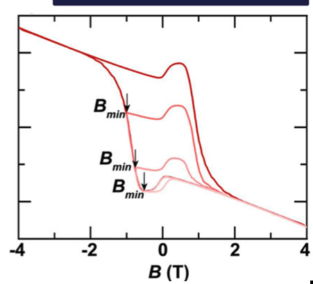
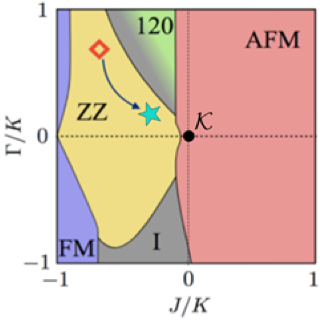
Hump in Hall Measurements Insufficient as Evidence for Skyrmions (MIP #87)
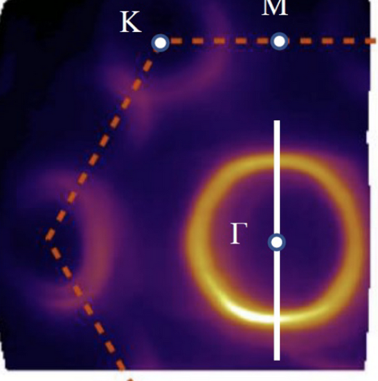
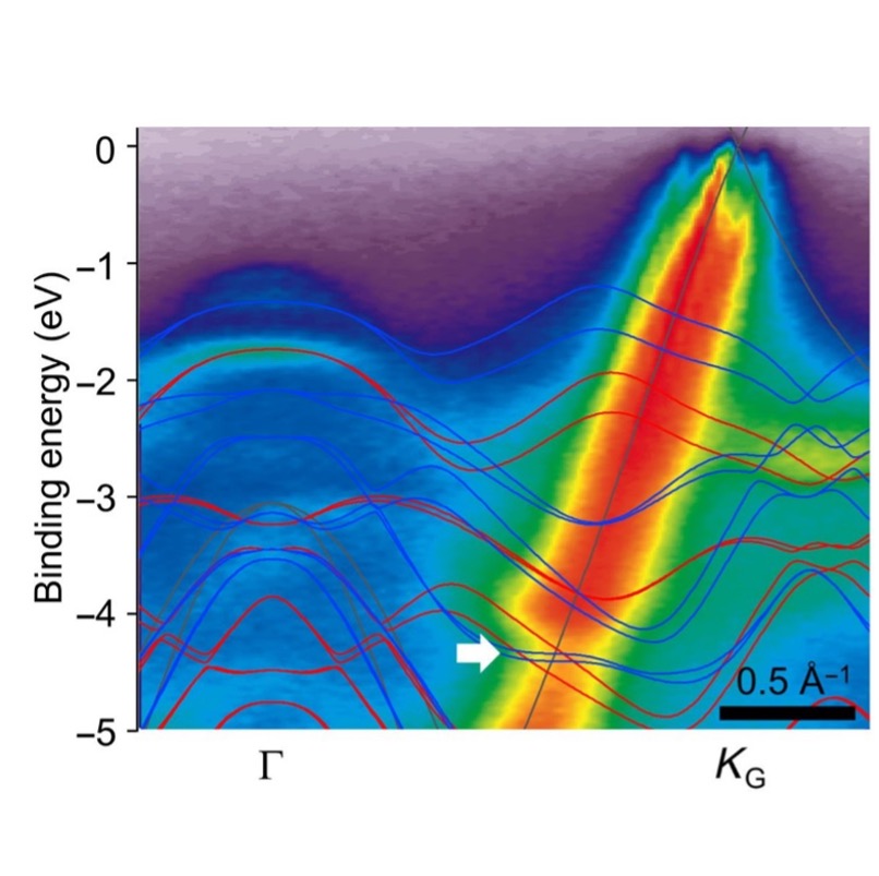
Expanding the Capabilities of Lab-Based ARPES on Quantum Materials (MIP #79)
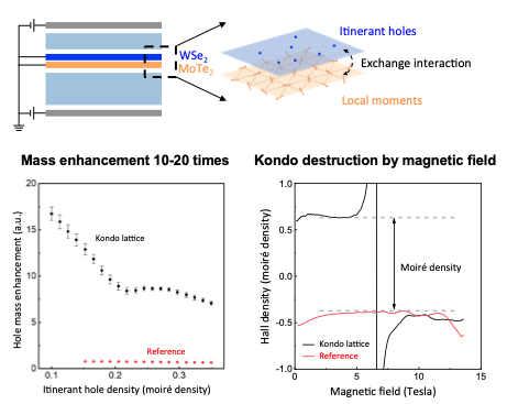
Gate-tunable heavy fermions in a moiré Kondo lattice (MIP #74)
The Electronic Phase Diagram of Moiré Superlattices (MIP #68)
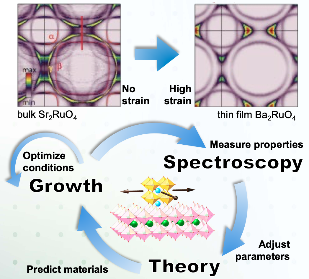
From Machine Learning to Discovery of New Family Member (MIP #66)
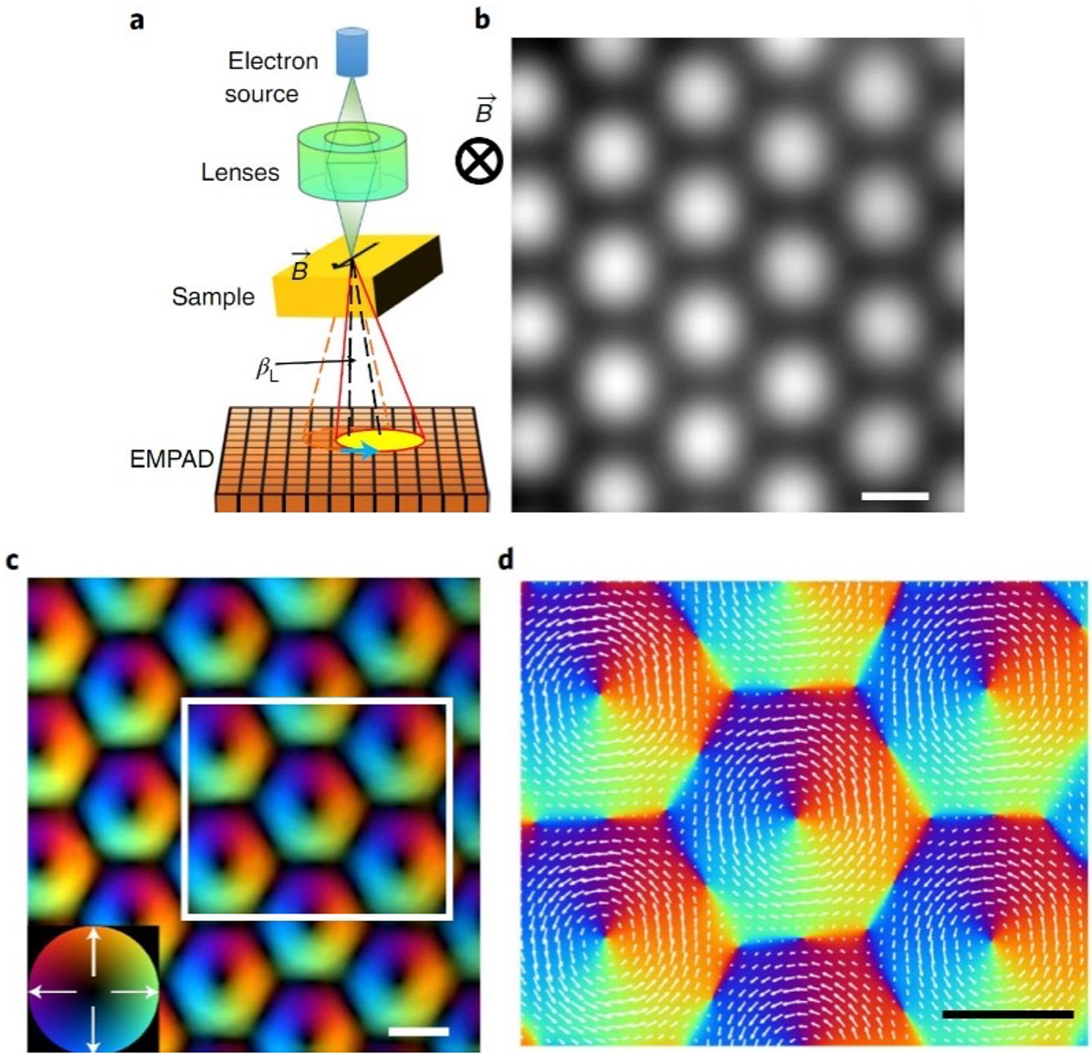
Lorentz Ptychography for high-resolution, high sensitivity magnetic imaging (MIP #65)
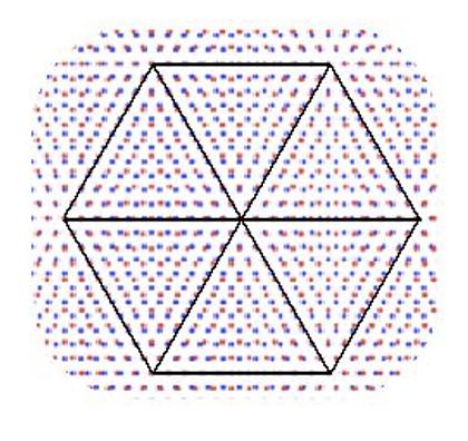
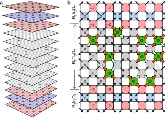
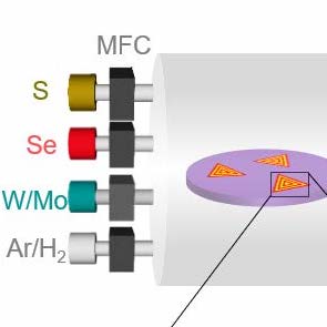
Engineering Quantum Fabrics with Arbitrary Periodicities (MIP #62)
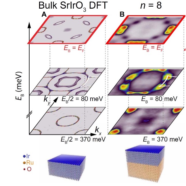
Metallicity of Ultrathin SrIrO3/SrRuO3 Heterostructures (MIP #60)
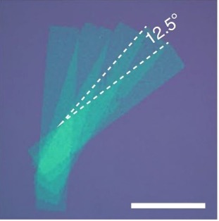
Robotic Assembly of Quantum Fabrics from Atomically Thin Layers (MIP #58)
Cleaning up a Quantum Material: from Quantum Enigma to Quantum Oscillations (MIP #48)
Quantification of Interfacial Electron-Phonon Coupling from Photoemission Replica Bands in a High-Tc Superconductor (MIP #46)
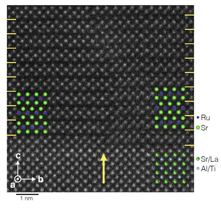
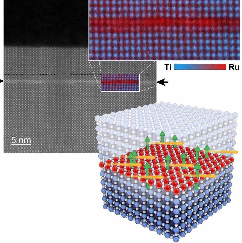
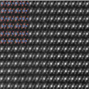
Cryo-STEM Unveils Electronic Order at the Atomic Scale (MIP #45)
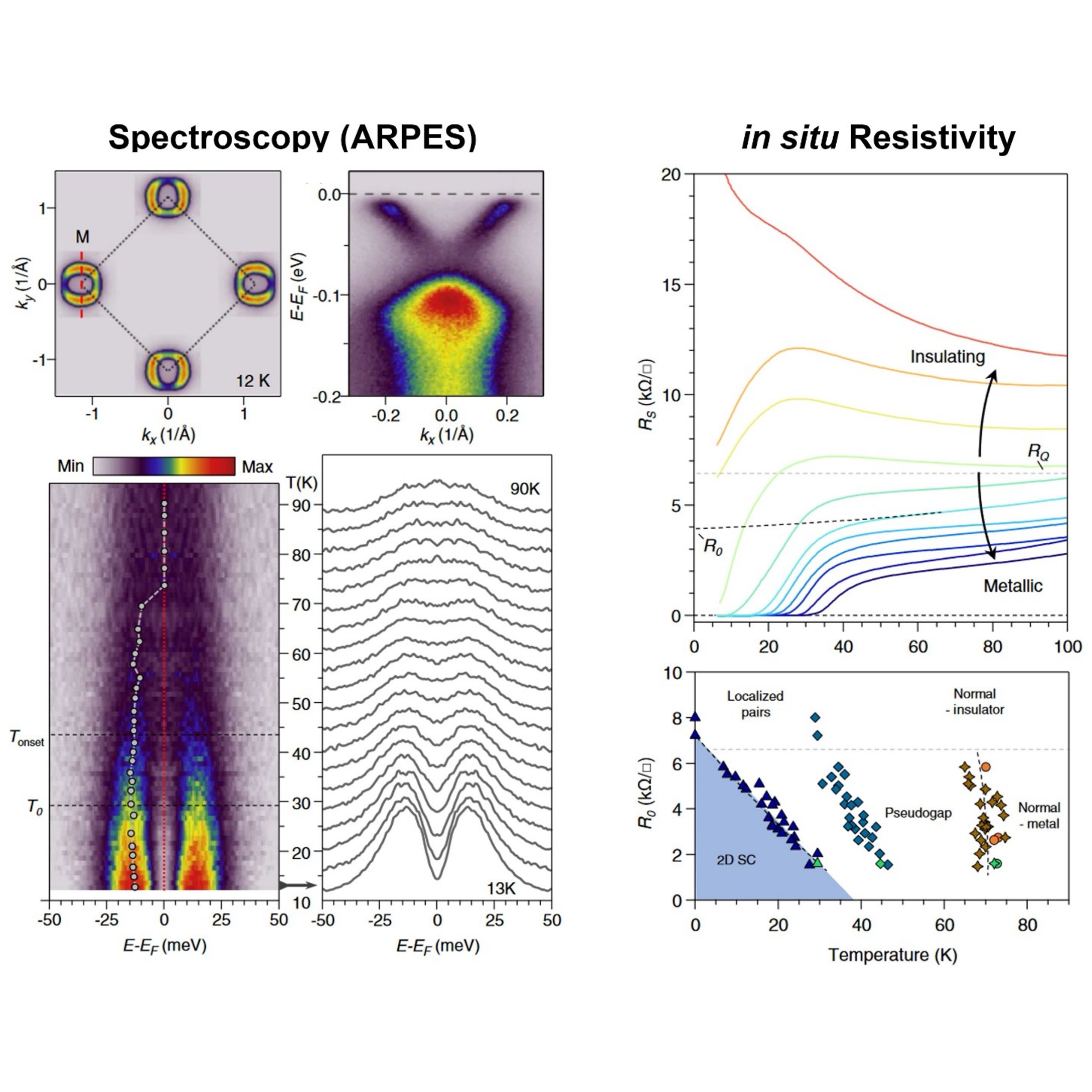
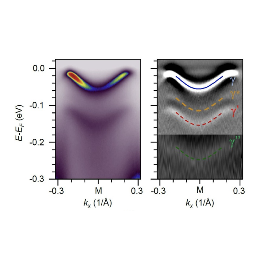
Discovery of “Pseudogap” Behavior in a Monolayer Thick High-Temperature Superconductor (MIP #43)
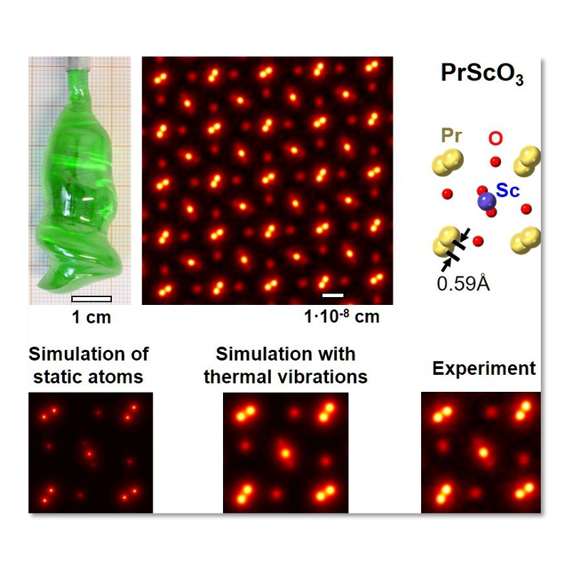
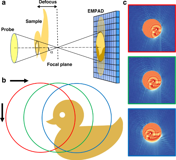
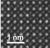
The Highest Resolution Microscope, enabled by a new detector technology, reaches an ultimate resolution limit – the vibrations of atoms themselves (MIP #42)
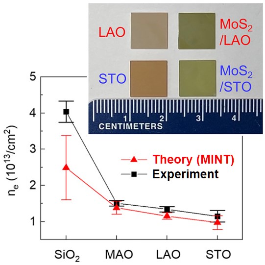
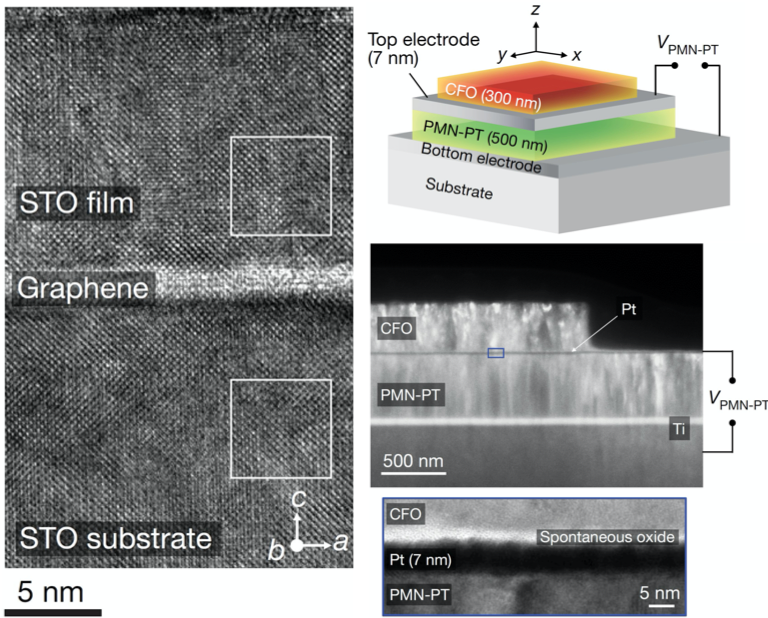
When Seemingly Passive Substrates are Active (MIP #37)
“Band-Structure Engineering” of Quantum Materials to Create a new Superconductor (MIP #36)
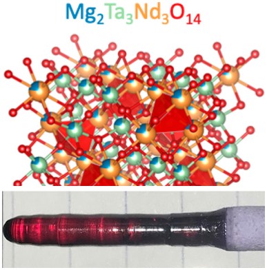
Discovery and Single Crystal Growth of High Entropy Pyrochlores (MIP #34)
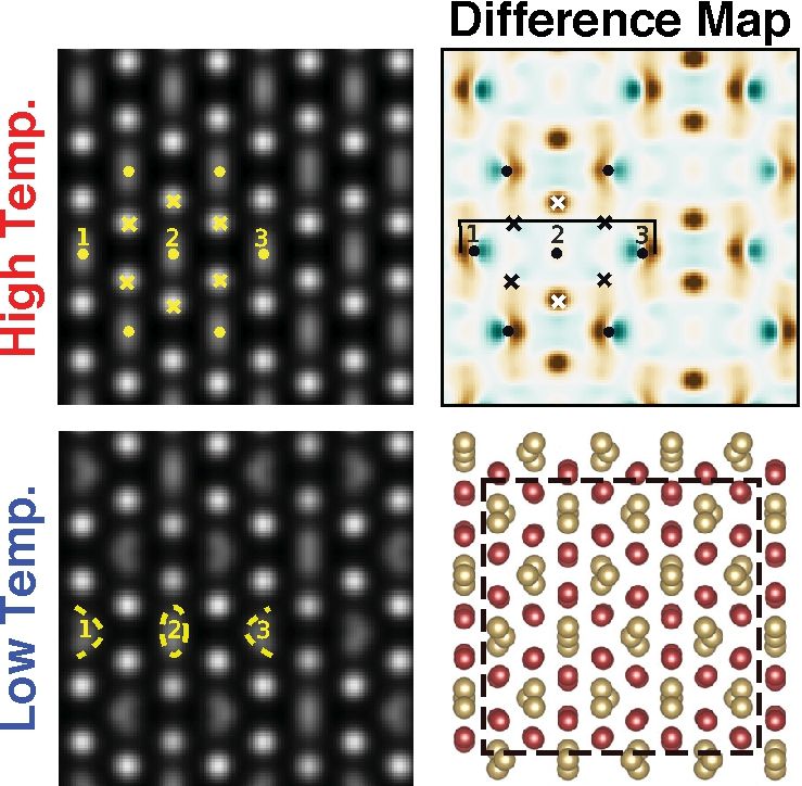
Atomic-Scale Visualizations of Low-Temperature Phase Transitions (MIP #33)
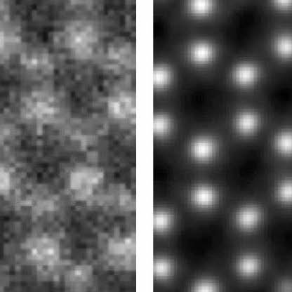
When it Comes to Seeing Atoms, Blurrier is Better (MIP #27)
New Sample Holder for High-Resolution Electron Microscopy at Previously Inaccessible Temperatures (MIP #24)
A Strategy to Make and Manipulate Magnetic Monopoles by Exploiting Interfaces (MIP #23)
New theoretical approach to tackle interface quantum materials (MIP #22)
PARADIM machine learning model for assisted optical floating zone synthesis(MIP#21)
Freeing wafer-scale stacking of single crystals from the shackles of epitaxial constraints (MIP# 20)
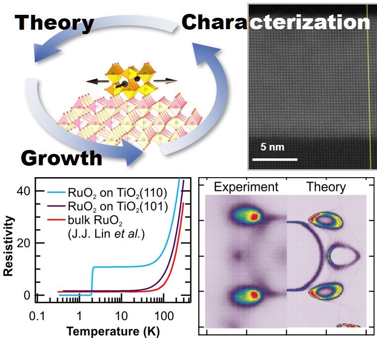
Theory+MBE+ARPES to navigate correlated materials A new Modality of Materials Discovery (MIP #16)
An atomically thin ferromagnet—just one atom thick (MIP #12)
Pushing boundaries: High pressure, supercritical optical floating zone materials discovery (MIP #11)
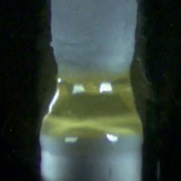
Superconducting Sr2RuO4 Films— key step toward ground-state quantum computing (MIP #10)
High-Resolution Electron Microscopy gets Cooler Sub-Angstrom Imaging at Cryogenic Temperatures (MIP #8)
New Detector for Electron Microscopy enables analysis of 2D Materials at record resolution (MIP #6)
Stretching Valleytronic Materials far beyond Conventional Limits to Tune their Properties (MIP #5)
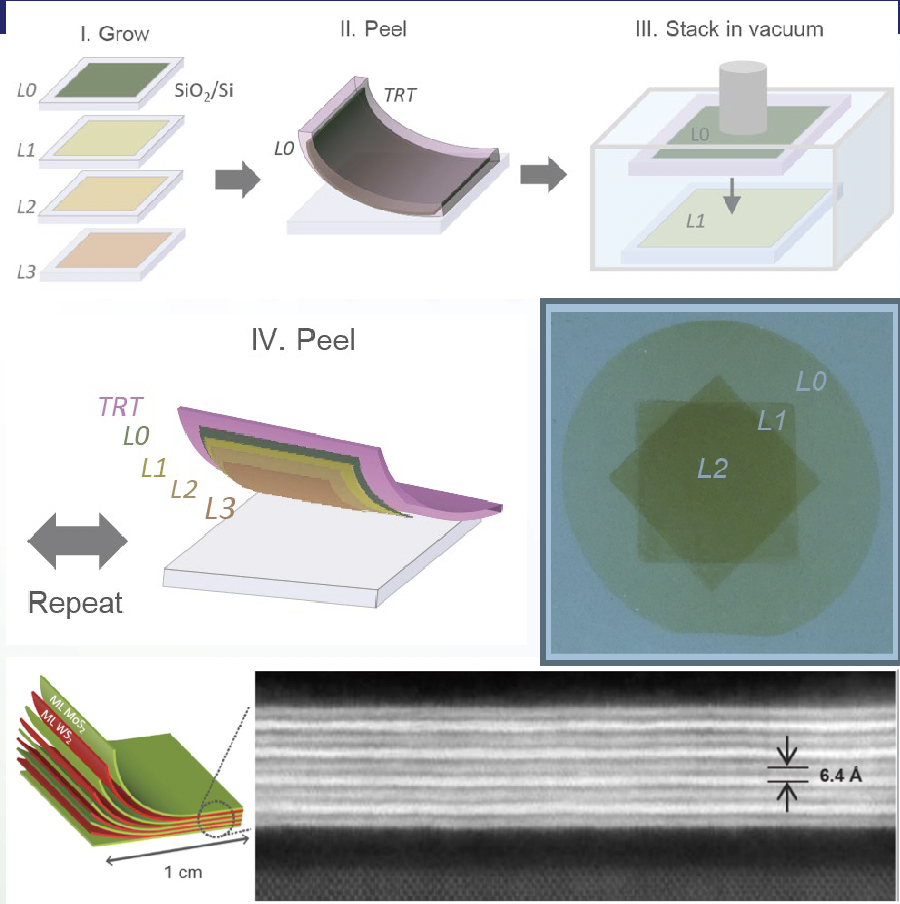
Valleytronics Made to Order: Layer-by-Layer Stacking of TMD Sheets with ~cm Dimensions(MIP #4)
Perturbing Valleytronic Materials to make them Relevant to Ground-State Quantum Computing (MIP #3)
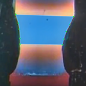
World-record high pressure floating zone crystal growth (MIP #2)
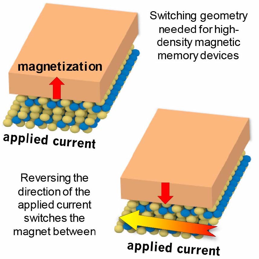
Low Symmetry Valleytronic Materials Enable Energy Efficient Switching for Magnetic Memories (MIP #1)